2D: Experiment That Was Labeled “Impossible” Until Now
By Nitai Garg · · 626 words
Topics: Physics, Tech, 2D, 2D Metals, AI Chips, atom, atomic, CHINA
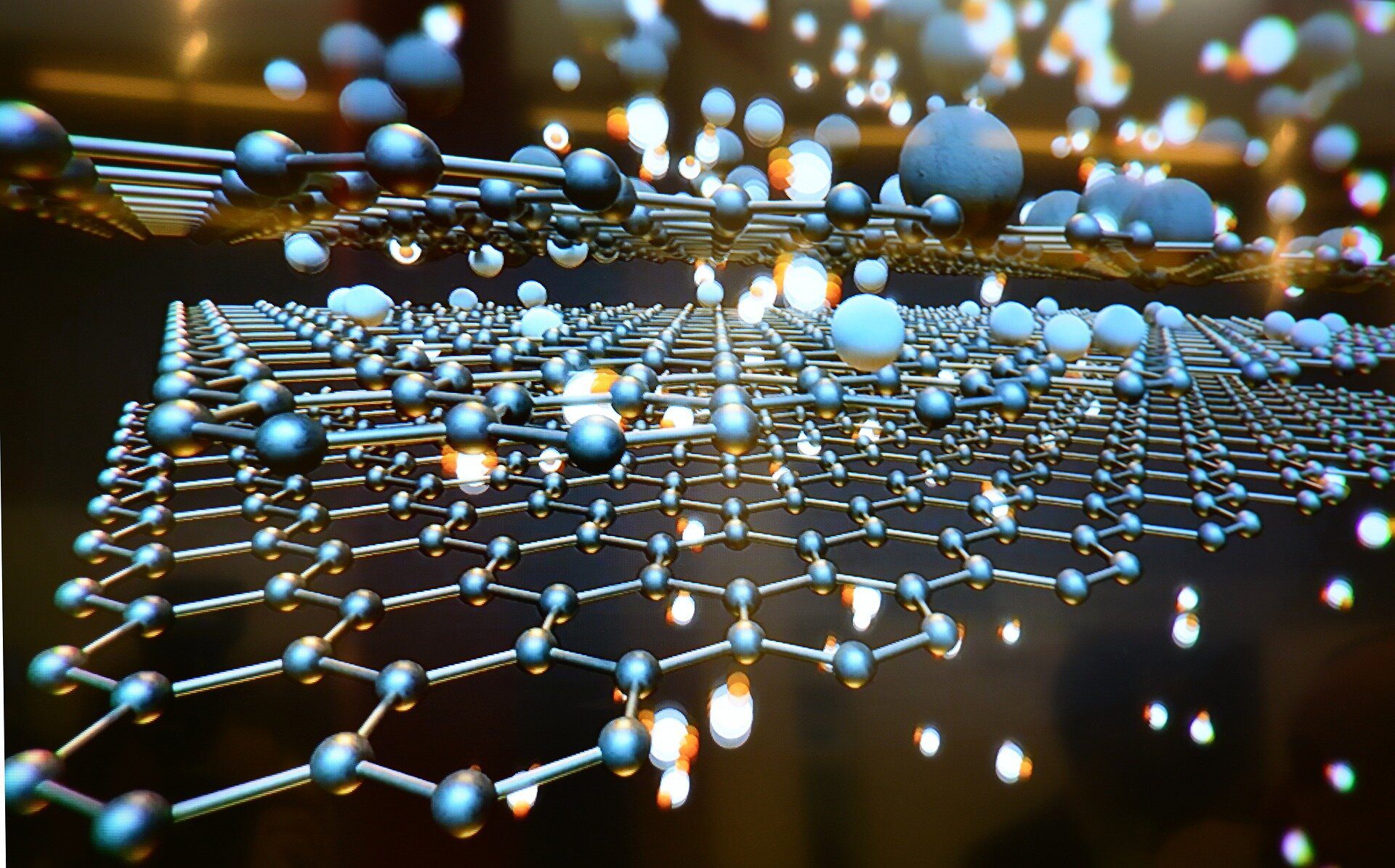
In the real word, any object you see, you feel, you touch is 3D, for example: a sheet of paper. Realistically 2D objects aka having only 2 dimensions, which are, length and width are purely theoretical and do not exist in the real world. Thus science tries to research on practical 2D objects, as these practical 2D objects due to the electron being confided in a place due to a process called quantum confinement, may show new sci-fi properties.
The concept of practical 2D objects have vastly been debated. While different opinions, scientists have agreed that a layer 1-3 atoms thick can be considered a practical 2D object. But its existence was again theoretical due to sheer amount of unstability which would cause the thin layer into curl up into a ball just like how water droplets tend to form a ball in pan.

Until March 2025, when a team of researchers led by Prof. Guangyu Zhang and Luojun Du at the Institute of Physics under the Chinese Academy of Sciences (CAS) published their landmark findings in the scientific journal Nature. This is considered breakthrough of the year 2025 as it was thermodynamically impossible to achieve.
They accomplished this by using a ground breaking technique called van der Waals (vdW) squeezing.
Think of it like making a smash burger, but on an atomic scale:
- The Atomic Buns: They take two plates of sapphire coated with a single layer of a material called molybdenum disulfide (MoS₂). This material is atomically flat, slick, and incredibly strong.
- The Patty: They put normal metal powder (like tin, bismuth, or lead) in between the plates.
- The Grill: They heat up the setup until the metal melts from powder into a liquid droplet
- The Smash: A machine presses the plates together with a force of 200 Megapascals (which is roughly the pressure of 2,000 atmospheres, or the weight of an elephant standing on a postage stamp).
- The Freeze: While keeping that crushing pressure active, they let the metal cool down. Because it is trapped between the two ultra-flat plates, it has no room to ball up which was the main problem. It is forced to freeze into a perfectly flat sheet just 2 atoms thick.

Added benefit: The atomic buns(MoS₂) stay attached to the ultra thin metal preventing it from rusting when it comes I contact with oxygen just like electroplating. These ultra flat metals show zero performance degradation for a full year under ambient environmental conditions.
| Metal | Size |
| Tin(Sn) | ~5.8 Å thick (~2 atoms thick) |
| Bismuth(Bi) | ~6.3 Å thick (~2 atoms thick) |
| Lead(Pb) | ~7.5 Å thick (~2-3 atoms thick) |
| Indium(In) | ~8.4 Å thick (~3 atoms thick) |
| Gallium(Ga) | ~9.2 Å thick (~3 atoms thick) |
Why this is big?
•Topological Insulators: The ultra thin tin works as a piece wood inside but like a wire with zero electrical resistance on its outer edges, meaning no energy is wasted as heat dissipating increasing the efficiency of all circuits
•The Silicon Saviour: Computer microchips are currently reaching their physical limits because anymore reduction in size leads to silicon transistors overheating too fast.These 2D metals can create microscopic, atomic-scale electrical wires and switches that don’t heat up, allowing for faster, smaller computers.
•The Ultimate Sensors: Since the metal is ultra thin(1-3 atoms thick) any small object such as a protein or virus will instantly change electric current.Potentially diagnosing the issue and thus useful in medical research and diagnosis, as well as environmental sensors.
These concepts can be used in elevating technologies such as quantum computing, new gen microchips, ultra-sensitive sensors etc.